Description: Project to use ATMega32's inbuilt timer to switch on/off an LED.
This is one of the simplest projects (like a 'Hello World') using a microcontroller.
Objective is to learn:
- Using ATMega timer output wave (instead of toggle of a GPIO pin) to blink an LED
- PCB design (using Kicad, trying fabrication company)
- PCB soldering (through-hole components in smaller places)
- Formulate an overall process for upcoming projects
- Creating repository of useful links and learnings for future reference - in a connected story type format
- Breadboard & wires
- Wall socket to convert 220v ac to 12v dc (used 12v DC to simulate car environment)
- Voltage converter 12v to 5v dc: L7805cv (datasheet)
- Button to switch power on-off: 6 pin, DPDT (working as per gif below)
- LED to show power status on/off: clear blue color
- Resistor for power LED: 100 ohm resistor (since clear blue led consumes ~3V)
- Power supply stabiliser capacitors: 10uf (voltage capacity >=12V) - 2 pc
- [optional] Power module: DC2DC step-down converter - 12 to 5v (used only initially for stable power on breadboard)
- ATMega 32a (PDIP package) microcontroller
- ATMega programmer (usbasp)
- Decoupling capacitors : 0.1 uF, voltage capacity>=5v - 2 pc (Paper on choosing de-coupling caps - relevant for high speed systems but good to know)
- Reset resistor: 10k ohm (ATMega design consideration document recommends this value)
- Switch button for reset: 2 pin, SPST (simplest possible push button, can go for 4/6 pin)
- Red LED (consumes ~2V)
- Resistor for LED 150 ohm (since red led consumes ~2V, if other color, choose resistor that satisfies V/R=20mA approx )
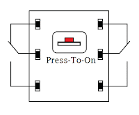
6 pin DPDT button
Software
- AVR-GCC (c compiler, using v4.8.1, link for latest)
- AVR dude to push hex file to microcontroller (using v6.0.1, link for common commands)
- Makefile in TextEdit (helpful video)
- AVR Libc (using v1.8.0, full library, IOheaderfile)
- R studio (to write C program)
C program logic
- Define pin PB3 (OC0) as output - since this is the default pin for 'timer 0' to send it's output wave
- Set timer/control register in CTC (clear timer on compare match) mode (page 81 of datasheet) - In this mode, the counter is cleared to 0 when the counter value matches the value in a particular register (OCR0)
- Enable interrupts - global and CTC
- Set counter start and end value (254 in our case)
- When you give power, microcontroller runs the program, timer starts from 0 and increments by 1 every clock pulse. With a prescaler of 256, timer clock pulse slows to 1MHz/256. So, one clock pulse = 256 us.
- When counter reaches 254 (the end value), a CTC output match interrupt is generated. The interrupt toggles the OC0 pin (output pin connected to LED). With each toggle of this pin, LED switches on and off - creating a blinking effect.
- Timer takes 256*255 (=65) us to count from 0 to 254. This is half cycle of the square wave generated. LED stays ON for half cycle and OFF for another half.
- 1 blink = 1 cycle of the square wave generated. It takes 2*256*255 us = 130 mS.
- After 5 blinks (10 interrupts), timer frequency is toggled between 256 and 1024 prescaler. LED blinks with two different frequencies - toggling every 5 blinks.
Steps
- Read complete ATMega32 datasheet
- Leave microcontroller fuses as default (clock 1MHz)
- Write C program and makefile
- Compile (make compile .c—>.hex etc)
- Push to micro controller (make flash)
Paper circuit
Only the pins that are used, nearest to the component they are connected to. No need to match physical layout.

Working prototype on breadboard


Breadboard to PCB
1. Design (on paper)
2. Create symbols (lib editor)
Most symbols are present in existing Kicad library. Downloaded digikey library for the switch symbol.
3. Schematic capture (eeschema)
Can draw only the pins that are used, can place them nearest to connecting component. Instead of matching physical features. This makes the schematic light, clean and easy to understand.
 |
| Schematic in Kicad (eeschema) |
4. Create footprint (footprint editor)
Most footprints were available in Kicad. Just had to create one for 2-pin push button - used existing 4 pin one and deleted 2 pins. The associated 3D symbol was left as-is. To create 3D symbols, FreeCAD.
5. Generate netlist (cvpcb)
Auto-generated netlist must be reviewed carefully and simplified to look like the schematic.
6. Board layout (pcbnew)
This is where everything comes together including drawing of tracks.

7. Generate gerbers (gerbview)
Sanity check everything thoroughly by switching on / off the various layers.
8. 3D view
Excellent view to check the sanctity of the board at various stages.
 |
| 3D view - top |
 |
| 3D view - side |
 |
| 3D view - back |
PCB design learnings
- Thick vs thin tracks: current capacity should be considered to choose thick / thin track. In this project, we used thick tracks for power (12/5V) travelling till a point where we know the current will be less (due to the component constraint - microcontroller in this case).
- Auto-generated nets are sometimes un-intuitive: things are in parallel but sequence also matters (ex. stabiliser capacitor should come first). Auto/technical nest will not necessarily take care of this.

Power line after de-coupling capacitor - Design Rule Check (DRC) error: pads are too close. capacitor footprint (4mm*1.5mm). Tried ‘update footprint from library’ but no use. When compared the instance (in circuit) with template footprint, template pads look much smaller. In instance, the pads are overlapping big time, in template they are not. Solution: There are three things: drill hole, copper pad and clearance. The template shows only the pad and drill hole. The instance (in circuit), it also shows clearance. The clearances were overlapping big time. there was a ‘very small’ overlap between ‘pad’ (copper) boundaries - just a tiny touch. Moved one pad with 3 keystrokes (at 0.1 mil grid) and they are separated. No error from DRC. Such a tiny shift should not cause any problem in actual board.
 |
| Capacitor footprint from template - no apparent problem |
 |
| Capacitor footprint from circuit (shows overlap between pads) |
Actual PCB
 |
| As received from fabrication company (LionCircuits) |
Soldering
Arranging components to solder
Bend leads so they are stable
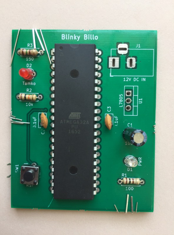


For microcontroller, only the pins that are used (6 in number) are soldered.
The board worked in first instance of supplying 12V power through jack barrel.


 |
Two boards soldered for practice - both worked |
- Place the components tightly before applying solder, especially the bigger ones, once soldered they will stay where they were e.g. one of the barrel jacks remained slightly above the board - not ideal.
- Voltage converter and barrel jack were bigger components. They did not have large leads to bend / does not allow the board to be flat while soldering. Hence, they were soldered at the end. Note the voltage converter is bent in one of the boards (going outside the board border) and standing on the other. Not much impact here but think about orientation before hand.
Link to next project: LCD
Absolutely amazing work both of my you! Super proud ! Best wishes
ReplyDeleteVery impressive,i like the details you provided in different forms. Good luck!
ReplyDeleteMaking from scratch is really a big achievement!